| PCM-X3 Processor Development Blog updated: 2022/12/03 09:32:51 +0200
Video output of encoder displayed on monitor. 29/04/2020
Early PCB Prototype 18 February 2020 decoder I'm resurrecting this project and have been doing a lot of thinking and reading. I'd like to use the following circuit to recover the system clock from the video tape. The recorded clock bursts are applied at J5 so that the PLL can sync and lock. An alternative is to record a 44100Hz/8=5.5125kHz tone on the linear sound track and apply that to J5. This can be used as a reference for the circuit below to generate a 22.5792MHz or 11.2896 MHz system clock.
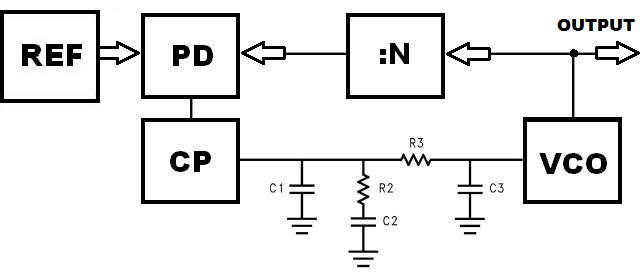
Source ti.com 1 March 2020 decoder The following circuit is simpler and does not require tedious and complicated programming of the CDCE913.
14 March 2020 Got some very nice prototyping boards.
Right-Click open image in new tab 20 March 2020 Calculating the PLLPRE, PLLDIV and PLLPOST settings for a recovered clock (from DIR9001) of 128 x fs. Doing it graphically like below helps a lot. Divide by 28 so set PLLDIV to 26. (offset of two for some reason)
26 March 2020 The whole country is going into a 21 day lockdown today, which gives me plenty of time to work on the PCM-3. I have to original code running on the PIC just generating the sync pulses for now using the onboard RC clock so the frequencies are still off. The waveform shapes are correct though. Next, I have to wire up the SPDIF interface.
28 March 2020 Day two of lockdown. Got the SPDIF receiver working. Now to clock the dsPIC from the recovered SCKO at 256xFs. 29 March 2020 Day three of lockdown. The dsPIC is now running using the recovered system clock from the DIR9001 at 39.51 MIPS. At this speed the video lines are slightly longer, but not so that it would cause sync problems. 40 vs 39.51 MIPS is a 1.2% difference making a 64us line, 64.8us long. Next is connecting the Data Converter Interface (DCI) and the Serial Peripheral Interface (SPI). 30 March 2020 Day four of lockdown. The dsPIC is doing some weird things. There is an output on the SPI iterface, but not entirely what is expected. It is like all "ones" is always read in or something. The data pattern on the SPI remains unchanged, but when STOP is pressed on the CD player, it goes to zeroes with only the clock run-in showing. I'm stuck! I don't know if the samples are being read into RAM correctly, since my old ICD2 don't want to seem to "Run the Target" in DEBUG mode. So I can't read the FIFO RAM contents. It's just fighting me so badly. I don't know what to do next.....
Above and Below: Sync pulse at top with SPI output below. Different scales.
It occurred to me that I'm essentially implementing an asynchronous FIFO in software. Since I'm stuck with the current build, I have decided to "re-imagine" the PCM-X3 and implement the FIFO functionality in hardware using a 1K x 9 (CY7C425) Asynchronous FIFO chip. I'll use the chip as a serial shift register reading samples in at one rate and clocking them out at another. The dsPIC will still generate the video sync, but will now be used more as a controller, housekeeper and signal generator and supervisor. Let's see what happens! Building on the breadboard will allow me to try the DCI and SPI on the dsPIC one last time also.
Above: PCM-X3 encoder re-imagined. CS8412 digital audio receiver, CY7C425 Asynchronous FIFO and dsPIC33. 31 March 2020 Day five of lockdown. Construction of the new PCM-X3 is progressing well. The SPDIF receiver is working. I'm busy wiring up the dsPIC33. IT WORKS! Well sort of. It only runs from a 20MHz crystal. For some reason it won't run from the MCK provided by the SPDIF receiver. I'm investigating.
Above: PCM-X3 encoder producing video lines with audio data. All processing is being done on the dsPIC33. The external FIFO memory wasn't needed. 1 April 2020 Day six of lockdown. IT WORKS! Seriously, everything works now from the appropriate clock source. I discovered a limitation on the input oscillator frequency when running in EC mode with PLL. The input clock is now 5.6448MHz or 128 x Fs. I also had to use a 74HC04 as level translator between 5V --> 3.3V and a 74LS74 as clock divider 256 x Fs --> 128 x Fs. I'm also over clocking the PIC very slightly.
The design of the encoder unit is actually very simple. All of the complexity is in the software. The CS8412 is configured for I2S audio data output format. This is fed to the DCI of the dsPIC33. The SPI interface output produces the data stream which must be merged with the sync pulses on RG0. The dsPIC33 is configured for external clock mode with PLL. The 256 x Fs = 11.2896MHz output clock (MCK) of the CS8412 is divided by two using the 74LS74 to get 128 x Fs = 5.6448MHz. This is fed to the CLKIN pin of the dsPIC33. All other ground and power connections as per the data sheets. Revisited the VCO calculations for 11.2896MHz for the decoder unit.
2 April 2020 Day seven of lockdown. I added the analogue output stage of the encoder unit. It now produces a single properly formatted video signal. Below is the video signal and left to right, the sync pulse, clock run-in and PCM audio data. The clock run-in has been changed to 1010101010101010. The run-in will later be applied at the decoder to a 4046 PLL to extract the system clock.
3 April 2020 Day eight of lockdown. I connected the encoder circuit to a monitor. Click on the image below for a video.
Changed the code to reduce the clock run-in frequency so that it can be used as reference for the decoder 4046 PLL. Changed my mind and changed it back again after doing my maths. Eliminated blank lines at bottom of frame. I'm busy developing and testing the clock recovery sub-system for the decoder unit. It involves using a 555 in monostable mode to generate a gating pulse to isolate and remove only the clock run-in from the video line. The 555 is triggered using the line sync pulse. It then stays "high" until just after the clock run-in is complete, thereby isolating it for application to the 4046. Changed number of active storage lines to 294
The video above shows the video output with the low frequency clock run-in still in place, but now you can see and hear the relationship between the sound and the video output. I'm using an old computer monitor with green phosphor. Tré cool! Below is the gating pulse from the 555 and the isolated clock run-in from the data stream (left). Also below is the first part of the video data frame and the isolated clock burst. (right) This setup will be used in the decoder unit to feed the 4046 PLL and PIC24 clock supervisor/extractor.
4 April 2020 Day nine. I did some calculations for the VCO in the decoder below:
l might be using a PIC as a phase comparator and a DAC to generate the VCO control voltage. I have not had success with a conventional 4046 PLL setup. The digital technique is ultimately more reliable and controllable. Let's see. 6 April 2020 Day eleven. I'm developing the decoders' clock recovery system. I'm testing a PIC24 to generate a PWM signal proportional to the phase difference between the 4046 RC oscillator and the incoming clock reference bursts from the video tape. The PIC24 will act as a phase comparator and generate the frequency control voltage for the 4046 via a low-pass filter. Testing and configuration continues. Below from left to right is the 4046, PIC24, 555 and an AND gate. The output from the 4046 VCO and the clock bursts from the AND gate will be applied to the PIC24. These will generate interrupts and based upon the relative timing of these interrupts, the PIC24 will either increase or decrease the duty cycle of the PWM output signal. This filtered PWM control voltage will then be applied to the VCO to pull the PLL into lock.
Below is the code sequence used to map a peripheral to an output pin on the 28 pin PIC24 I'm using. This code sequence is vital and the main reason I haven't been able to get the 28 pin dsPICs working. I tried using the built-in unlock routine of the compiler, but it didn't work so I did it manually. I followed the datasheet very literally and it worked!
Mapping a peripheral to an output pin on the PIC24 10 April 2020 The lockdown has been extended to 30 April and I'm slowly getting sick of it now, but I'm still playing with my circuits. I'm still testing and contemplating clock recovery from the data stream. Using the PWM module on the PIC24 I can generate a control voltage for the 4046 VCO, but there is still a lot of noise on the filtered PWM output, which concerns me. Another option is to use a DAC. To that end I'm testing an old R2R ladder DAC. The idea is that a DAC like this would have a clean static output voltage. I have ordered three dsPIC33FJ128MC804 chips. These actually have a stereo DAC onboard. My hope is that the onboard DAC would be able to generate a nice clean control voltage for the 4046 VCO. Another benefit would be that I can simplify the decoder hardware having a smaller chip (44 pin vs 100 pin) and also a stereo DAC onboard, thereby eliminating one chip. Below left top to right to bottom: DAC output, dsPIC and DAC, Burr-Brown DAC700BH
The dsPIC is generating a ramp of 0000 to FFFF and back down again. The output on the DAC700 swings between 0V and about 10V. 13 April 2020 I've had some very moderate success with the PLL, but accurate locking is still an issue. I've decided to use the VCO on the 4046, but implement the leading/lagging comparison on the PIC24. To that end I have been divising an algorithm to determine if an input signal is lagging or leading a reference signal.
I create a "measurement window" using the timer interrupt. During this "window" I wait to see which signal has the first rising edge. Depending on which signal has the first rising edge, either the VCO or the reference, I can determine if the VCO is leading or lagging the reference signal. I shall code this tomorrow and see what happens. 15 April 2020 After much struggling and asking on forums, below is a confirmed working code example of INT1 being used to trigger on the rising edge of an input signal on pin 17 of a 28 pin dsPIC33FJ128GP202. This should also work on a PIC24. Notice the IOLOCK lock/unlock sequence for the PPS (Peripheral Pin Select) pin assignment. This works with the XC16 compiler hence the use of <xc.h.>
above is the external INT1 being triggered during the data frame clock run-in Now that I have an interrupt service routine triggering at the right time, I can write the software to determine which of two signals is lagging or leading. The paper design is shown under 13 April 2020. Once I am able to make a lead/lag measurement I can use a DAC to control the VCO in the 4046 to bring my local clock and the clock from the data frame (video line) into sync. This will then provide me with a local system and playback clock. Getting the clock out is a vital part of the decoder system and the only part that is really still an unknown. 18 April 2020 I have had some success measuring the period of the clock run-in an reproducing it using the PWM module. As can be seen below the period of the clock run-in and the PWM signal is the same although there is a curious variability in the phase or something. Picture taken off of the screen of a 30 year old digital scope meter. I need to freeze the signals to check them. Look towards the right and you'll see the two signals' periods line up although I'm not sure what's happening on the left. I'm hoping there is a variability in the RC clock I'm using on the dsPIC at the moment. I should "close the loop" and have the PIC measure the PWM output and the clock run-in and match them.
20 April 2020 Whoohoo! Got the analog PLL working thanks to some online calculators. Below are the values I used. the circuit and the scope trace. I learned so much in the process of making this PLL. I'm using a 2nd order loop filter now since it is quicker to build.
21 April 2020 Another clean PLL lock! The clock reference is highlighted in yellow with the PLL VCO output below. Frequency is 1.2348MHz, C1=6.8pF, R2=150K, C2=22pF, Charge Pump Current = 0.3mA, Kvco=0.017394MHz/V. VCO section R1=220K, R2=14.5K, C1=470pF.
clock reference lines up with VCO output, R2 = 14.7K 24 April 2020 I connected up another dsPIC in decoder configuration, feeding it the data frame and sync pulse from the encoder unit. I also added a TDA1545 DAC. I'm getting an output stereo signal, but there are some anomalies that'll have to be debugged. At least I have it 95%. Below, the decoder unit with DAC is in the top left corner with the rest of the board occupied by the encoder unit. The experimental PLL is bottom right. I have learned a lot in the last month and also brushed up on my coding and debugging skills. Overcoming the engineering challenges one by one has increased my confidence. We're still in lockdown and it's challenging building this system since I have to scavenge parts sometimes.
25 April 2020 I have a theory as to what is happening. The decoders' FIFO buffer runs dry because it is too small, 1024 bytes. Considering that one TV frame stores 294 x 6 = 1764 bytes, 1024 bytes is too little to compensate for the gaps in the data stream between fields. I also just can't make the FIFO buffer bigger. I'm using DMA to write the audio data out to the DAC so as not to interrupt the SPI process. DMA memory space is only 1024 words (16 bit). If I forego DMA I run into trouble with SPI and DCI fighting for CPU time. I may have to ditch DMA and try to overclock the dsPIC. This problem may take some time to figure out. I'm going to pause the project here. Due to the lockdown I cannot get the components I need to go further. I'm planning to build hardware implementations of both the decoder and the encoder because right now it's a case of software. I feel the hardware has been sorted out. 28 April 2020
Video of decoder sound output showing phase distortion most likely caused by buffer under-run
30 April 2020 PROGRESS!! I'm busy testing the decoder by reading stored samples from RAM as if it was using a FIFO buffer with sound samples. Previously I had not been able to run the DCI and SPI concurrently in the decoder circuit when using normal SRAM instead of the DMA RAM. Tweaking the interrupt priorities seemed to do the trick, but I now have to test to see if it'll read in audio samples correctly.
SPI Read clock (top) from the decoder neatly aligned with incoming data signal (bottom)
Output from DAC. There is no actual break in the signal it is the camera shutter.
SPI Read clock (top) neatly aligned with incoming data signal (bottom). There is a ghostlike signal at the top that could indicate an instability. 2 May 2020 Fiddled a bit with code. No progress. 3 May 2020 While meditating it occurred to me that instead of adding another level of complexity with the decoder board Mark 2, let me first re-factor my existing code to streamline it. I have a number of while loop polling states that take place. I want to remove these and replace them with interrupts. That way I can free up CPU cycles and perhaps get the system to work without DMA and using regular SRAM for the FIFO buffer. 7 January 2022 I want to attack this project again but this time using the much faster dsPIC33CK32MP506 at 100MIPS instead of 40MIPS. Stay tuned.
Current development prototype with SPDIF interface (bottom left), encoder (middle), decoder (top) and DAC (top middle). PLL play area (bottom right) and a sprinkle of 74 gating and control logic. 11 January 2022 Ordered four dsPIC33CK256MP206 chips and TQFP adapter boards. 27 January 2022 My new dsPICs arrived.
13 November 2022 Here we go boys and girls! Hang on tight! I really think I can get it working with the new generation of dsPICs. The only problem I had, the only one, was buffer under-run because I was forced to use DMA. The DMA RAM space in the PICs I was using was 1024 bytes. That's it! Problem is, one video field contains 1764 bytes, followed by a gap where the VBI is. Bottom-line, the buffer was just too damn small and I got gaps in playback. With the new PICs you can define your own DMA RAM space inside the 24K system RAM. As much as you like! No more being stuck in a corner. Also they run at 100MIPS instead of 40. I was totally maxing out the previous dsPICs at 40MIPS. I'm also considering introducing VITC SMPTE timecode using the ICS2008AV.
Top right TDA1545 Stereo DAC and Burr-Brown OPA2134 SoundPlus Op-Amp. Two dsPIC33s and the DIR9001 SPDIF reciever
| ||